Hypercube Developer Website
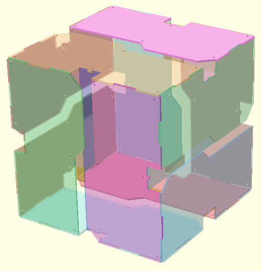
Hypercube Geometry 
- Do you see all 12 PCBs in the translucent diagram above? :)
- Note a complete mirror image assembly is also possible by flipping each board to its reverse side. Take care when assembling boards to use the above configuration.
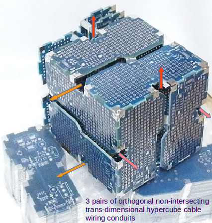
- This diagram shows the 3 pairs of orthogonal conduits used for wiring a Hypercube in 3D
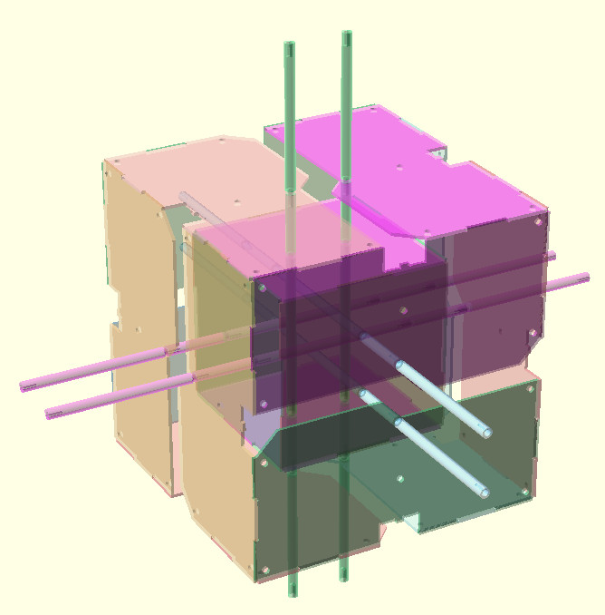
- The Hypercube can be assembled by soldering the corners of PCB to save costs.
- A better way is to assemble the Hypercube to an inner cube made of PCB or acrylic
- The internal cube can instead be another onion layer of Hypercubes. Many such layers can be packed together depending on space constraints, wiring constraints and thermal constraints.
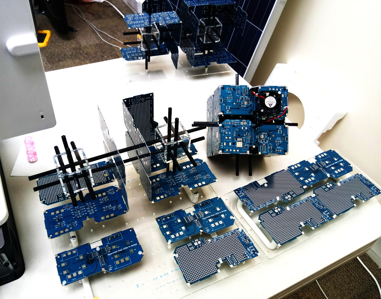
- The diagrams can look complex, in practice it is easy and very compulsive assembling Hypercube boards :)
- More information here about lever cam mechanism for locking the spacers