List of Hypercube open source boards
All boards here will at some stage become open sourced along with its software
- Additional Open Sourced Support Boards
- We are designing a set of 3D printable and laser cut boxes for the Hypercube boards - all to be open sourced
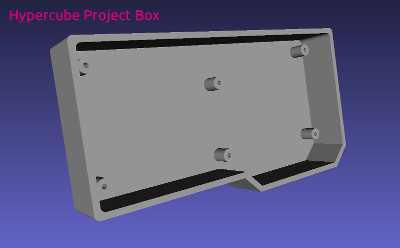
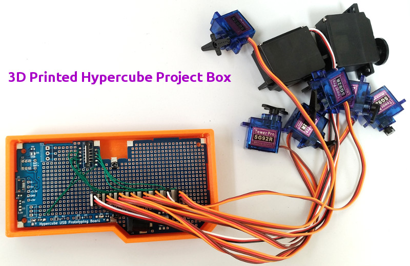
- The box has been successfully 3D printed and tested as a case for a Hypercube board as shown in above picture. Two screw holes in center hold the board with 4 screw holes at the outer edges for the lid.
- The lid can be made by 3D printing, but as it is flat, the lid is more quicker to design and make with laser cut acrylic.
- This type of flat acrylic lid can have numerous openings and holes for items such as switches, LEDs, control knobs, pots, wires, displays and so on. With laser, engraved lettering is also possible.
- The case needs holes on the side walls for connectors (if fitted). This is easier to do after the case is printed rather than try to put the holes into the case at design time which make printing difficult with supports (unless you got a dual head 3D printer that has option for dissolvable ink such as PVA).
- More on 3D Printed Cases...
- Eventually all the boards will become available in one single KiCAD project with a sheet for every supported Hypercube board
- From there you can design any kind of new product using real Hypercube boards and rewiring as needed, and draw its circuit by connecting the KiCAD sheets that are in use for your design.
- Then you can lay out the PCB, or give it to us to make it for you.
- The software libraries we do as well, and it will be proper multi-tasking code that you can just keep adding to make all the supported boards work together well. See the Hypercube Software section for more details.
Developer Services For Startup Companies
- Finally, as a service, we also develop boards and software, or get partially finished software and hardware working for startups based on equity or fixed price. The above technologies are examples of what we can do.
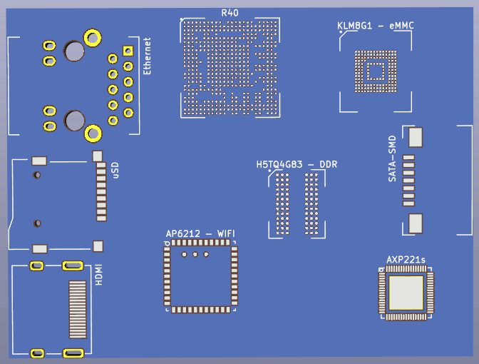
Open Source Linux Allwinner R40 ARM SoC Board
- KiCAD based Linux ARM SoC boards are now under development. These boards are open sourced with more to come in the future. The plan is:
1.Create a verbatim copy of an existing open sourced board (BPi board in this case) that is based on Allwinner R40 SoC chip
2. Add modifications to create a custom minimalist server board
3. Layout simple board with RAM CPU and essentials to boot Linux
4. Layout the complete board and boot Linux on to it
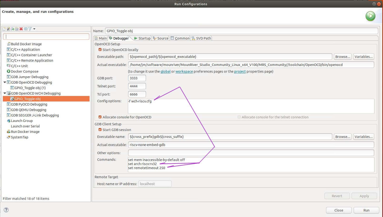
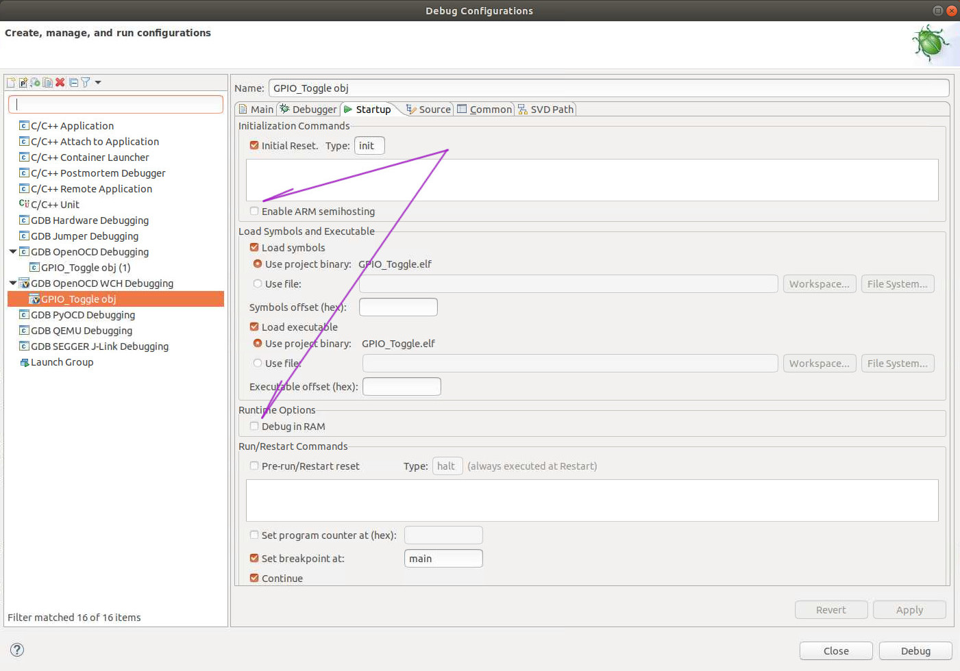
KiCAD Notes
To open the KiCAD file in a fresh install of the latest KiCAD, the home directory ~/.config/kicad has two files fp-lib-table and sym-lib-table that seems to be out of sync with the rest of the software installation.
This will manifest itself in a lot of files not being found when KiCAD library editor or PCB footprint editors are run.
To work around the problems, rename those two files to save them, and copy in the file same two files in /usr/share/kicad/template directory to the ~/.config/kicad directory and then restart KiCAD. You may still get one or more errors, but those are down to errors with specific libraries and can be ignored.
The paths to R40 related schematic symbols (and later the footprints) will be in relative subdirectory libs from the project file directory. Wherever possible relative paths are used so that projects don't break when transferred to a new desktop setup in a different PC.
More information on fixing KiCAD errors
Install KiCAD5 BOM Generating Tool
- KiCAD5 BOM generator - https://github.com/SchrodingersGat/KiBoM
- The software has be downloaded to PC and the PC must have ability to run Python (Linux this is built in)
- Add the software to the Tools > Generage Bill of Materials.. dialog box (KiBOM_CLI) and run from there.
- The file is generated in the project folder e.g. cpu_board_bom_.csv. Open the file with comma as the separator to get correct BOM for the board.
- Manually edit the cells as needed. Alternatively, fix the issues in the Schematic and regenerate the BOM
Electronics Design Notes
- R40 board RAM data pins do not follow D0..D7 ordering - it is based on wiring convenience
- R40 RAM has DSQ DSQ- pins which are fed by 4 separate pairs SDQS0P SDQS0N, SDQS1P, SDQS1N etc, one for each chip
- Most of the resistors and capacitors are 0402
- All resistors should be 1%
- Some high value capacitors are 0603 and 0805
- Some 0R resistors are 0805
- Global labels and net labels are used to connect tracks together
- This design uses a lot of power supply labels
- The CPU is split into 12 parts - when generating the schematic symbol, specify that the symbols are not interchangeable
- Some clock wires have small capacitors (around 5pF) that can be inserted to correct clock skew
- The ESD diodes for HDMI have pairs of wires on either side that are internally connected. The pads for some reason have been numbered consecutively (it need not be in KiCAD as pads with duplicate numbers can exist in KiCAD)
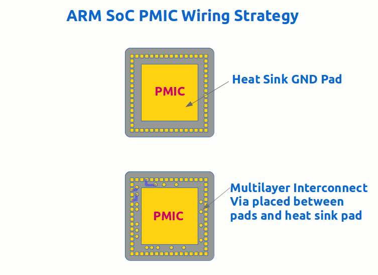
- Many tracks around the PMIC has width restrictions
- The main inductors around the PMIC are high current, low internal resistance 4x4mm SMD inductors
- The SMD MOSFET Q1 has pads under the chip that need to be wired
- The ESD diode has a + and - symbol to differentiate the two pins
- There are SATA, HDMI, USB, MIPI DSI wires that have differential drive that requires length tuning to make it work correctly, and the wires need to be kept parallel and together to prevent noise and reflections.
- The pull up resistor for the eMMC should be close to the eMMC pins to reduce the chance of picking up noise
- The DDR address and data lines should be length tuned but it does not say that anywhere
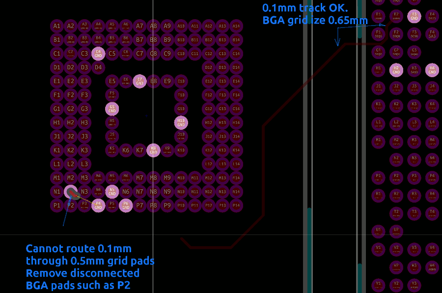
- Example SA0 (F6 on BGA) from Allwinner R40 goes to A0 (K3 on BGA) on all 4 DDR chips. The wiring for that would look something like the drawing below. Every path from the CPU to DDR is same length. The tolerance is about +/-0.3mm or better for GHz operation. The minimum trace widths are about 4 mils or about 0.1mm to get wires in and out of BGA pads of the R40 CPU. This makes them more expensive to fabricate than the usual 6 mil widths and clearances for normal PCB.
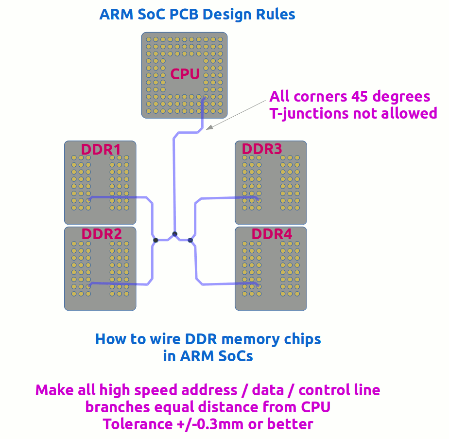
- When calculating the length of tracks where layers are crossed, remember to take account of the layer thickness! If the PCB is 1mm thick, and there are 6 layers, then crossing each layer will cost 0.167mm. Sometimes it is best to list the tracks in a spreadsheet and keep a record of each length that has been added. Because it is the total that matters it is possible to get the cells to highlight themselves if the total lengths are not within spec.
- When routing 0.1mm wires through BGA pads, the Allwinner R40 CPU pad spacing is 0.65 mm and routing is easy. However the BGA pads of the flash is 0.5mm and the BGA pads are too close to allow a 0.1mm wire to be routed through the gaps. In this instance, a limited number of unconnected BGA pad(s) such as P2 are removed from the footprint to gain access to the pads that are isolated.
- The PMIC has most of its multi layer vias placed behind the pads in the gap with the thermal heat sink pad. That saves a lot of wiring space.
Layer Organization
- Layer 1 = signal
- Layer 2 = GND plane
- Layer 3 = signal
- Layer 4 = signal
- Layer 5 = 3.3V power plane
- Layer 6 = signal